Média
Nanoelectronics – The miniaturizing principle

Big things are happening at small scales. Electronics makers are learning to build devices with features just a few atoms across. This will not only make computers even more powerful and energy efficient, but will pave the way for entirely new types of electronic devices. The impact of these innovations could change lives across the world.
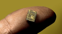
Imagine a complete clinical diagnostic testing laboratory in a disposable box the size of your thumb, or spectacle lenses that not only display tomorrow’s weather forecast on demand but also charge your cell phone battery. Devices like these are just some of the possibilities enabled by nanoelectronics – an approach that exploits the unique properties that emerge when materials are shaped and combined at the tiniest of scales.
“Nanoelectronics involves devices which have features less than 100 nanometers in size, and where that feature size defines the functionality of the device,” explains Professor Jo De Boeck, Ph.D., Chief Technology Officer and Executive Vice President of Imec, a Belgian nanoelectronics research center. 100 nanometers (nm) is very small indeed: one ten thousandth of a millimeter, around the size of a flu virus. “Down at that scale, you see dramatically different characteristics,” continues De Boeck. “You see quantum effects. You can tweak the electrical properties of materials or shift the wavelengths of laser light.”
Today’s mainstream electronic devices sit firmly in the nanoelectronic space. The most advanced integrated circuits (IC), or computer chips, consist of billions of transistors with features 25 nm across or smaller.
“Nanoelectronics has already changed our lives,” says De Boeck. “It is the reason we don’t burn our hands when we make a call on a modern cell phone, and that we have very high resolution displays on our mobile devices and laptops.”
Indeed, our ability to engineer objects with features 1,000 times thinner than a human hair has arisen largely as a consequence of more than half a century of evolution in the power and efficiency of the integrated circuit. “Moore’s law”, proposed in 1965 by Gordon Moore, cofounder of Intel Company, stated that the number of transistors that could be squeezed onto a single integrated circuit would double roughly every two years.
Since then, the industry has continually found ways to meet Moore’s predictions, by adopting new materials and new manufacturing techniques that allow it to cram ever more and smaller components onto a silicon wafer. Today’s stateoftheart integrated circuits have features only 22 nm across, and researchers are working on designs half that size again. As they start to include features just a handful of atoms in size, however, they are coming up against some hard physical limits.
Pushing the limits

“There are three ways that manufacturers can increase the performance of chips,” says Claus Poppe, Vice President of Electronic Materials at BASF. “The first is shrinking the transistor size. This is what Moore’s law is about. However, the industry accepts that 5 nm for the transistor gate length is as small as it can go, and it expects to get there in the next 10 years. The second way is to use new materials, like cobalt or germanium, to replace or augment the silicon used today. The third is in geometry, with the replacement of today’s basically two dimensionaldesigns with 3D ones.”
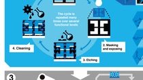
The industry’s ability to achieve its next evolutionary aims will depend in part on the right chemistry. The vast majority of steps in the 600 to 1,000 process cycles required to build a state of the art computer chip require chemical inputs and every evolution of the chip makes new demands on those chemicals. “As you get down to the nanoscale, our chemical knowhow becomes a key success factor,” says Lothar Laupichler, Senior Vice President, BASF Electronic Materials. One of his units – headquartered in South Korea – employs two thirds of the staff in the company’s worldwide electronics business, an indication of the signi ficance of Asia to today’s global IC business, and of the importance of close collaboration in developing increasingly tailored materials for it. “In order to achieve innovation at this nanoscale, you have to understand interactions at a molecular level which also demands an extraordinary degree of purity”, says Boris Jenniches, Vice President, Business Management BASF Electronic Materials Asia Pacific, and responsible for this unit.
Purity matters because, at the nanoscale, even a few stray atoms of the wrong material can make the difference between a working circuit and a faulty one. Checking that BASF’s electronic materials meet the cleanliness levels demanded by its customers is a key part of Jan Willmann’s role. He is Operations Manager at the Competence Center Analytics Clean Room Lab at BASF in Germany. “We are trying to detect contamination at levels of between 10 and 100 parts per trillion,” says Willmann. “That’s a level where, if you showed the sample to somebody in the pharmaceutical industry, they would say ‘we can’t see anything at all, this is perfectly clean’.”
Faster, cheaper, energy efficient
The ability to shape and manipulate materials with extraordinary precision at the nanoscale is creating opportunities in a number of areas beyond conventional chip design. Many of the key limitations of conventional batteries come from their physical construction. To build better batteries, engineers want to increase the effective surface area of the anode and cathode to make it easier for electrons to flow bet ween them. “Shaping the electrode surface in 3D at the nanoscale allows this to happen,” explains Philip Pieters, Business Development Director, Energy Technologies at Imec.
Researchers hope that such batteries will not only store more energy than conventional designs, they’ll also be much faster to charge, paving the way for electronic devices and even electric vehicles that can be recharged in minutes rather than hours. As well as nanoscale batteries, Pieters’ research team is working on high precision printing technologies that can be used to apply ultrathin layers of electronic materials in a range of other areas. Printable photovoltaics, for example, will eventually allow buildings to generate electricity from the sunlight falling on their façades and windows, or even from the otherwise wasted interior light hitting interior walls and ceilings.
“A diagnostic test that takes less than 10 minutes and costs less than $10 could transform healthcare in many parts of the world.”
Dr. Robert Bollinger, John Hopkins University
University of California Los Angeles’ spinoff Aneeve Nanotechnologies has developed an approach that allows electronic circuits to be printed onto a wide variety of substrates. “The printing process isn’t just cheap and energy efficient compared with conventional chip manufacture, it offers other environmental benefits too,” says Aneeve CEO Kosmas Galatsis. He says, the carbon nanotubes used by Aneeve are “safe, sustainable and earthabundant” compared to some of the rareearth materials like tantalum and indium required in much of today’s conventional electronics.
Aneeve’s approach allows circuits to be applied to transparent materials in such a way as to be invisible to the naked eye. The company hopes that this will dramatically reduce the cost of manufacturing robust, flexible displays or wireless communication capabilities. This could enable new wear able technologies, like glasses with built in displays that could offer an “augmented reality” experience: floating direction arrows to help navigate an unfamiliar city, say, or customer reviews and opening hours next to nearby stores and restaurants.
Seattle-based Heapsylon, a startup established by a group of former Microsoft employees, meanwhile, is taking a more intimate route, using nanoelectronics technologies to build sensors directly into clothing. Its products, which include pressuresensing socks for runners and bras and tshirts that can measure the wearer’s heart rate, are claimed to be soft to the touch and completely machine washable.
The lab on a chip

As well as taking integrated circuit manufacturing technologies into wider applications, nanoelectronics is being used to build entirely new capabilities into chips themselves. The same technologies that allow chipmakers to etch shapes and apply different materials to make transistors can also build tiny pipelines, minuscule sensors and miniature machines. Earlier this year, Imec entered a partnership with Johns Hopkins University in Maryland, United States, to pursue the development of nanoelectronic medical diagnostic systems. “We envision a device the size of a USB stick that could conduct many of the diagnostic tests that currently take place in laboratories,” explains Liesbet Lagae, manager of Imec’s life sciences program.
Using sensors embedded into chips, the Imec team hopes to be able to conduct an array of tasks, from pregnancy testing to the identification of antibodies for viruses like HIV and even the analysis of DNA. “We have all the basic building blocks in place,” says Lagae. “We understand the microfluidics so we can build tiny capillary pumps into our circuits that mean the sample effectively sucks itself through the chip. We can do PCR (Polymerase Chain Reaction), used to amplify DNA prior to testing. And we know how to integrate biomarkers into our circuits that generate an electrical or photonic signal when they are exposed to particular enzymes or antibodies.”
There is still work to do before the Imec Johns Hopkins team achieves its vision, however, and as with conventional chips, much of that depends on the development of the right chemistry. Integrating delicate biological molecules into chips remains extremely challenging. “We need to overcome issues of shelflife,” explains Lagae. “The biomarkers need to be stabilized so they don’t break down before use, and that hasn’t yet been done in the silicon environment.” There are manufacturing challenges too; several of the steps used to produce a conventional chip require the application of high temperatures, which could destroy delicate biochemicals.
“We envision a device the size of a USB stick that could conduct many of the diagnostic tests that currently take place in laboratories”
Liesbet Lagae, manager of Imec’s life sciences program
The long-term implication of nanoelectronics in biomedicine could be transformative, says Dr. Robert Bollinger, who leads the biomedical nanoelectronics program at Johns Hopkins University. “The ability to conduct testing at the point of care, wherever that is, will improve access to high-quality treatment and reduce the need for dedicated medical facilities.”
But it is the electronics industry’s ability to manufacture huge quantities of its tiny products cheaply that could really change the world. “Because nanoelectronics can make use of the manufacturing scale of the semiconductor industry, it creates the potential to deliver these capabilities at high volumes and very low cost,” says Bollinger. “A diagnostic test that takes less than 10 minutes and costs less than $10 could transform healthcare in many parts of the world.”
