Media
Press photos
In this area you can find our press photos.
Pictures of the month

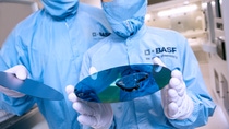
Chemical lab technicians inspect the surface structure of a silicon wafer. In the clean room laboratory, BASF experts carry out application tests in chemistry and in semiconductor surface conditioning. As a leading market player in Asia and Europe, BASF has strong expertise in delivering process chemicals and solutions for the semiconductor industry.

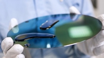
The lab technicians test the wetting properties of a silicon wafer after it has been treated with Planapur®, a polishing material that contains nanoparticles. Wafers are polished with Planapur® several times during manufacture. To ensure that no scratches develop on their surface, the grinding particles must be extremely small and fine. As a leading market player in Asia and Europe, BASF has strong expertise in delivering process chemicals and solutions for the semiconductor industry.

